
Fiber and Integrated Optics Laboratory
Integrated Photonic Devices
Integrated photonics is increasingly important because it enables the miniaturization and integration of optical components—such as lasers, modulators, waveguides, and detectors—onto a single chip. By manipulating light instead of electrical signals, integrated photonic systems can achieve extremely high data transmission speeds while consuming less power and generating less heat than traditional electronic circuits. This technology plays a critical role in modern applications, including high-speed data centers, telecommunications, quantum computing, sensing, and biomedical devices. In addition to improving performance, integrated photonics reduces system size, cost, and complexity, making advanced optical technologies more practical and scalable.
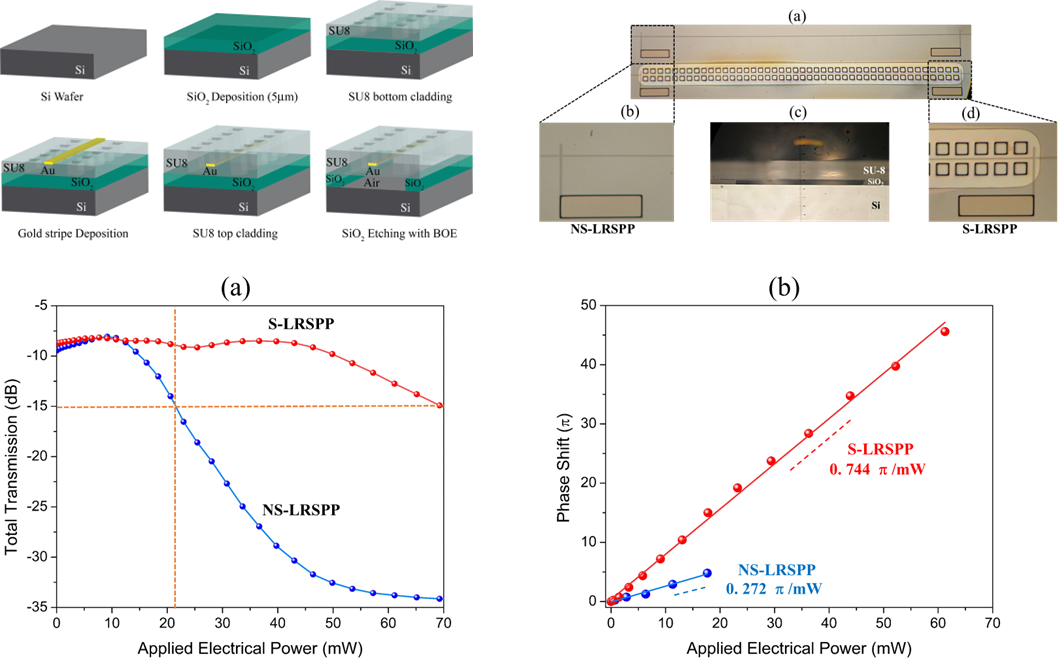
Long-range surface plasmon polaritons (LRSPPs) are electromagnetic waves that propagate along a thin metal film sandwiched between two dielectric materials with similar refractive indices. Unlike conventional surface plasmon polaritons, LRSPPs experience significantly lower propagation losses, allowing them to travel much longer distances along the metal–dielectric interface. This occurs because the electromagnetic field is more symmetrically distributed across the metal layer, reducing absorption within the metal. As a result, LRSPPs are particularly attractive for applications in integrated photonics, optical sensing, and plasmonic devices. Their ability to guide light at subwavelength scales while remaining compatible with photonic circuits makes them promising for compact optical communication and sensing technologies. We have demonstrated LRSPP on Si/SU-8 platform with a suspended geometry to reduce losses under active operation (electrical current heating), which can be ideal for the development of various active photonic devices. We are currently working to develop LRSPP-based biosensing applications.
InP (Indium Phosphide) multiple quantum well (MQW) switches and modulators offer several advantages, particularly in high-speed and high-performance optical communication systems. These devices leverage the quantum confined structure of multiple quantum wells to achieve efficient light modulation with low power consumption. One key benefit of InP MQW switches and modulators is their ability to operate at high frequencies, making them ideal for applications in dense wavelength division multiplexing (DWDM) systems, which require fast switching speeds and low insertion loss. In addition, InP's direct bandgap material allows for efficient interaction with light, improving device efficiency and reducing signal degradation. The compact size and integration potential of InP-based devices enable highly scalable solutions for photonic circuits, contributing to the miniaturization and cost-effectiveness of communication systems. We have designed and fabricated devices for telecom applications based on selective area zinc-in diffusion based on MQWs.
We will pursue the design, fabrication, and testing of photonic devices based on other platforms (silicon and polymers), with the aim of developing research on areas such as Terahertz and integrated biosensors. We are currently working on LRSPP for biosensing and will continue to work with silicon and polymer platforms.